From contact lenses to latex gloves, technique prints flexible circuits on curved surfaces
Researchers from North Carolina State University have demonstrated a new technique for directly printing electronic circuits onto curved and corrugated surfaces. The work paves the way for a variety of new soft electronic technologies, and researchers have used the technique to create prototype “smart” contact lenses, pressure-sensitive latex gloves, and transparent electrodes.
“There are many existing techniques for creating printed electronics using various materials, but limitations exist,” says Yong Zhu, corresponding author of a paper on the work. “One challenge is that existing techniques require the use of polymer binding agents in the ‘ink’ you use to print the circuits. This impairs the circuit’s conductivity, so you have to incorporate an additional step to remove those binding agents after printing.
“A second challenge is that these printing techniques typically require you to print on flat surfaces, but many applications require surfaces that aren’t flat,” says Zhu, who is the Andrew A. Adams Distinguished Professor of Mechanical and Aerospace Engineering at NC State.
“We’ve developed a technique that doesn’t require binding agents and that allows us to print on a variety of curvilinear surfaces,” says Yuxuan Liu, first author of the paper and a Ph.D. student at NC State. ‘It also allows us to print the circuits as grid structures with uniform thickness.”
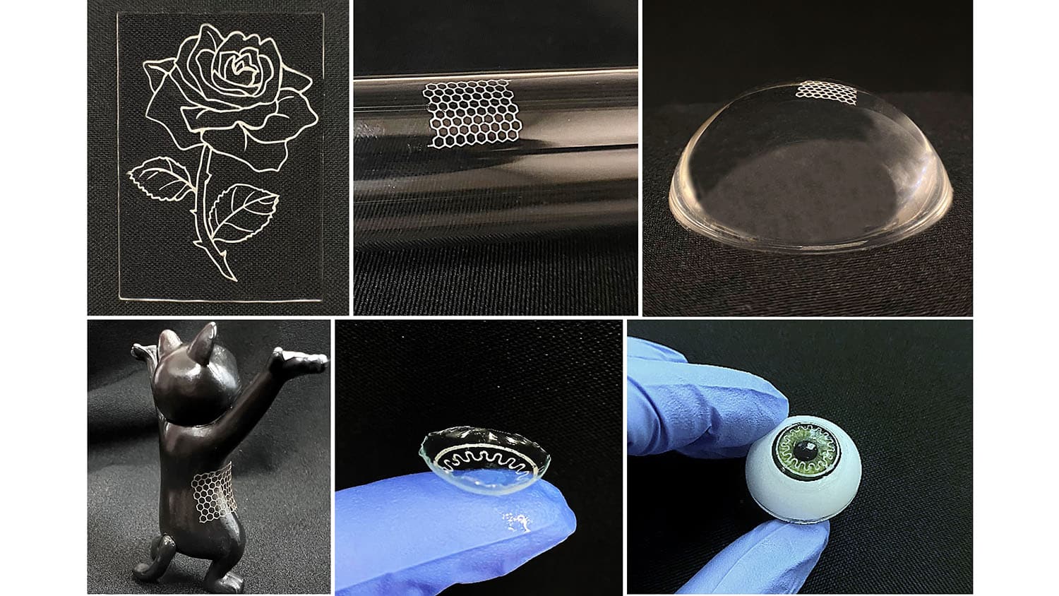
The first step in the new technique is to create a template for the relevant application that incorporates a specific pattern of microscale grooves. The template is then used to replicate that pattern in a thin elastic polymer film. Researchers then attach the thin polymer film to the relevant substrate, which can be flat or curved. At this point, the tiny grooves in the polymer are filled with a liquid solution containing silver nanowires. The solution is allowed to dry at room temperature, leaving behind silver nanowires in a soft material with the desired shape and circuit pattern.
To demonstrate the technique, the researchers created three proof-of-concept prototypes. One was a “smart” contact lens with built-in circuits, which could be used to measure the fluid pressure of the eye – which is relevant for some biomedical applications. One was a flexible, transparent electrode with circuits printed in a grid pattern, which could be used in solar cells or on touch panels. The third is a latex glove that has circuits printed on it that serve as pressure sensors, which has applications in robotics and human-machine interface applications.
“We think this could be scaled up pretty easily, in terms of manufacturing,” Zhu says. “We’re open to talking with industries who are interested in exploring this technique’s potential.”
The paper, “Curvilinear Soft Electronics by Micromolding of Metal Nanowires in Capillaries,” is published in the open-access journal Science Advances. The paper was co-authored by Brendan O’Connor, a professor of mechanical and aerospace engineering at NC State; Jingyan Dong, a professor in NC State’s Edward P. Fitts Department of Industrial and Systems Engineering; and Michael Zheng, an undergraduate at NC State.
The work was done with support from the National Science Foundation under grants 1728370 and 2134664.
-shipman-
Note to Editors: The study abstract follows.
“Curvilinear Soft Electronics by Micromolding of Metal Nanowires in Capillaries”
Authors: Yuxuan Liu, Michael Zheng, Brendan O’Connor, Jingyan Dong, and Yong Zhu, North Carolina State University
Published: Nov. 18, Science Advances
DOI: 10.1126/sciadv.add6996
Abstract: Soft electronics using metal nanowires have attracted significant attention attributed to their high electrical conductivity and mechanical flexibility. However, high-resolution, complex patterning of metal nanowires on curvilinear substrates remains a challenge. Here, a micromolding-based method is reported for scalable printing of metal nanowires, which enables complex and highly conductive patterns on soft curvilinear and uneven substrates with high resolution and uniformity. Printing resolution of 20 μm and conductivity of the printed patterns of ~6.3×10⁶ S/m are achieved. Printing of grid structures with uniform thickness for transparent conductive electrodes (TCEs) and direct printing of pressure sensors on curved surfaces such as glove and contact lens are also realized. The printed hybrid soft TCEs and smart contact lens show promising applications in optoelectronic devices and personal health monitoring, respectively. This printing method can be extended to other nanomaterials for large-scale printing of high-performance soft electronics.
This post was originally published in NC State News.
- Categories: